

The datasheet lists a gyroscope full-scale up to 4000 dps, an internal FIFO of about 9 kB and accelerometer full-scale options of 2/4/8/16 g — numbers that set system-level constraints. This article gives a concise, testable breakdown of electrical and sensor limits, recommended pin connections, and practical validation steps you can run on a prototype board.
1 — Background: LSM6DSRTR at a glance (purpose & place in IMU specs landscape)
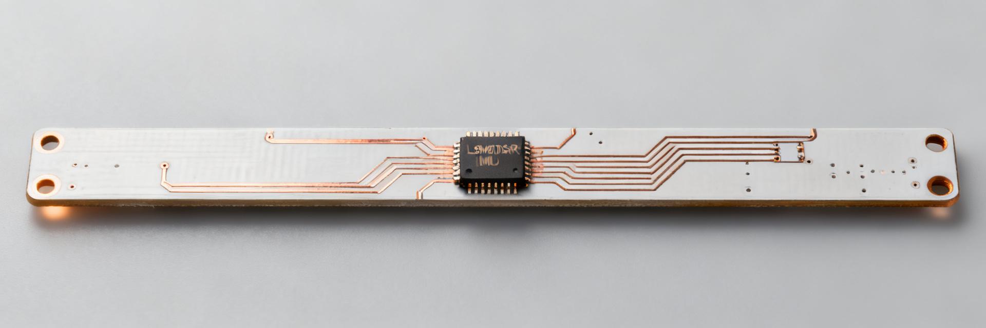
1.1 Core feature summary (what to extract from the datasheet)
Point: The device combines 3-axis accel and 3-axis gyro in a single package. Evidence: selectable accel FS (2/4/8/16 g), gyro FS to 4000 dps, and ≈9 kB FIFO. Explanation: these IMU specs make it suitable for motion sensing, gesture detection and low-power tracking; trade-offs center on range versus noise.
1.2 Package & typical system roles
Point: The part comes in a small multi-pin LGA package with an I2C or SPI host interface. Evidence: typical pin count fits microcontroller-domain placement. Explanation: designers place the sensor on the MCU power domain, close to the control MCU, mindful of mechanical placement to avoid vibration sources and torsion stress.
2 — Electrical limits & operating conditions for LSM6DSRTR
| Parameter | Operating Limits | Absolute Maximum | Unit / Condition |
|---|---|---|---|
| Supply Voltage (VDD) | 1.71 to 3.6 | 4.8 | V, relative to GND |
| I/O Voltage (VDDIO) | 1.62 to 3.6 | 4.8 | V, independent interface |
| Operating Temperature | -40 to +85 | -40 to +125 | °C, baseline range |
| Active Current (High-Perf) | 0.55 (typ) | 0.80 (max) | mA, Accel + Gyro on |
2.1 Supply rails, IO levels and absolute maximums
Point: Supply ranges and IO tolerances define interface safety. Evidence: design operating supplies conservatively below absolute max; treat VDDIO and VDD independently. Explanation: plan at least a 10% safety margin under absolute maximum ratings and avoid applying 5 V to non-tolerant pins; verify with your board-level power sequencing.
2.2 Power modes, current draw and thermal limits
Point: Current consumption varies strongly with mode and output data rate. Evidence: normal, low-power and sleep modes show different typical and peak currents and FIFO activity increases dynamic draw. Explanation: measure current with a bench supply and fast logging multimeter; account for thermal derating if ambient exceeds the operating temperature range to avoid drift or shutdown.
3 — Sensor performance: accelerometer & gyroscope IMU specs
3.1 Full-scale ranges, sensitivity, bandwidth and noise
Point: Choose FS and bandwidth to match motion dynamics. Evidence: per-LSB sensitivity shifts with FS (e.g., accel LSB to g conversion and gyro LSB to dps depend on selected range) and noise increases with bandwidth. Explanation: pick lowest FS that accommodates peak motion to maximize resolution and use lower bandwidth to reduce noise where latency allows.
3.2 Bias, cross-axis sensitivity, temperature behavior & calibration tips
Point: Bias stability and temperature coefficients drive calibration frequency. Evidence: datasheet lists bias drift figures and temp coefficients; a 0.5 mg bias translates to measurable position drift over seconds. Explanation: perform static zeroing, record bias versus temperature and apply simple linear compensation; re-run calibration after mechanical changes or long-term drift detection.
4 — Pinout deep-dive: key pins, functions & recommended connections (pinout)
4.1 Power, ground, decoupling and recommended PCB land pattern
Point: Proper decoupling and ground strategy are mandatory for stable operation. Evidence: recommended bypass caps and close placement to VDD/VDDIO pins reduce supply noise. Explanation: place 0.1 µF and 1 µF caps within 1–2 mm of pins, use multiple ground vias, keep traces short, and follow a single-point sensor ground to minimize induced errors.
4.2 Interface and control pins: I2C/SPI signals, CS/SA0/INT/FIFO lines
Point: Interface pins require passive components and routing discipline. Evidence: SCL/SDA or SCLK/MOSI/MISO/CS lines need pull-ups/pull-downs and optional series resistors. Explanation: use 4.7–10 kΩ pull-ups for I2C, 22–100 Ω series resistors for SPI lines to damp ringing, route interrupt lines to fast MCU pins and avoid long stubs that invite EMI.
5 — Hardware limits & protection: ESD, voltage transients, mechanical & soldering constraints
5.1 ESD and over-voltage protection recommendations
Point: Exposed comm lines and I/O require protection on fielded devices. Evidence: datasheet specifies ESD thresholds and absolute input limits. Explanation: add input clamps or small TVS diodes on external connectors and series resistors on comm lines for battery-powered or outdoor designs to limit transient currents and protect the sensor.
5.2 Mechanical mounting, solder reflow and thermal stress considerations
Point: Mechanical stress and reflow profiles affect reliability and performance. Evidence: vendor guidance lists acceptable soldering profiles and recommends keepout areas around the die. Explanation: use symmetric placement to balance stress, follow the recommended reflow curve, and avoid placing heavy components or fasteners near the chip to reduce bias and mechanical coupling.
6 — Testing & validation checklist: how to verify IMU specs on your board
6.1 Bench verification tests (what to measure and expected outcomes)
Point: Structured bench tests confirm electrical and sensor specs. Evidence: measure supply current per mode, read raw registers, convert LSB to physical units, and exercise FIFO depth. Explanation: sample at documented ODRs, compute RMS noise over a fixed sample set, and verify FIFO empty/full thresholds match expected byte counts for pass/fail criteria.
6.2 Integration & firmware validation (data handling, filtering, and calibration)
Point: Firmware must initialize and monitor the sensor correctly. Evidence: verify WHO_AM_I, configure ODR/FS, enable interrupts and FIFO as required. Explanation: implement anti-aliasing filters, sanity checks for saturation, periodic calibration routines and logging to detect stuck FIFO or communication timeouts during integration testing.
Summary
- The LSM6DSRTR offers selectable accel ranges and a large FIFO, enabling burst captures and flexible trade-offs between dynamic range and noise; confirm range and sensitivity choices against your motion profile and sampling budget.
- Respect electrical limits: follow recommended VDD/VDDIO decoupling, keep traces short on power and comm lines, and design with a 10% margin under absolute maximums to protect the device and system.
- Validate on real boards with bench tests and firmware checks: measure mode currents, convert raw outputs to physical units, exercise FIFO and interrupts, and apply temperature-aware bias compensation for reliable results.
FAQ
How do I verify supply and IO limits on my board?
Measure supply voltages with a calibrated bench supply and multimeter under load, then compare to operating ranges. Use a current meter to capture mode currents and transient behavior during FIFO bursts. If any measurement approaches absolute limits, add margin via regulation or select level-shifting components.
What are quick tests to confirm accelerometer and gyro accuracy?
Record stationary samples to compute bias and RMS noise, then apply known rotations or drops of known orientation to validate scale factors. Convert raw LSB values using the chosen FS to g or dps and compare to datasheet typical noise and sensitivity for pass/fail decision criteria.
Which layout mistakes most commonly degrade IMU performance?
Long power or ground traces, lack of proper decoupling near VDD/VDDIO, and nearby switching regulators are primary culprits. Keep sensor traces short, use multiple ground vias, isolate the IMU from high-vibration components, and follow the recommended land pattern to minimize mechanical and electrical interference.
What is the recommended SPI vs I2C physical layer termination for LSM6DSRTR?
For I2C, use robust 4.7 kΩ to 10 kΩ pull-up resistors on both SDA and SCL lines. For SPI configurations operating at high clock rates, omit the pull-up resistors and place 22 Ω to 100 Ω series damping resistors close to the MCU driver pins to mitigate signal ringing and transmission line reflections.