

This compact, data-first guide helps embedded storage teams validate an eMMC 5.1 HS400-capable 8GB eMMC module quickly. HS400 offers a theoretical interface throughput near 400 MB/s; in typical low-to-mid capacity modules designers should expect peak sequential reads approaching the interface limit while writes and random IOPS vary by firmware and NAND generation. The goal here is a tight walkthrough of datasheet callouts, expected versus measured performance, reliability math, and an integration checklist to speed sample validation and procurement decisions.
All numeric guidance below is intended as an actionable checklist: extract exact package dimensions, voltage rails, and firmware feature flags from the official datasheet version referenced by your qualification team before production signoff.
KLM8G1GEUF-B04P: Product overview & key specifications (Background)
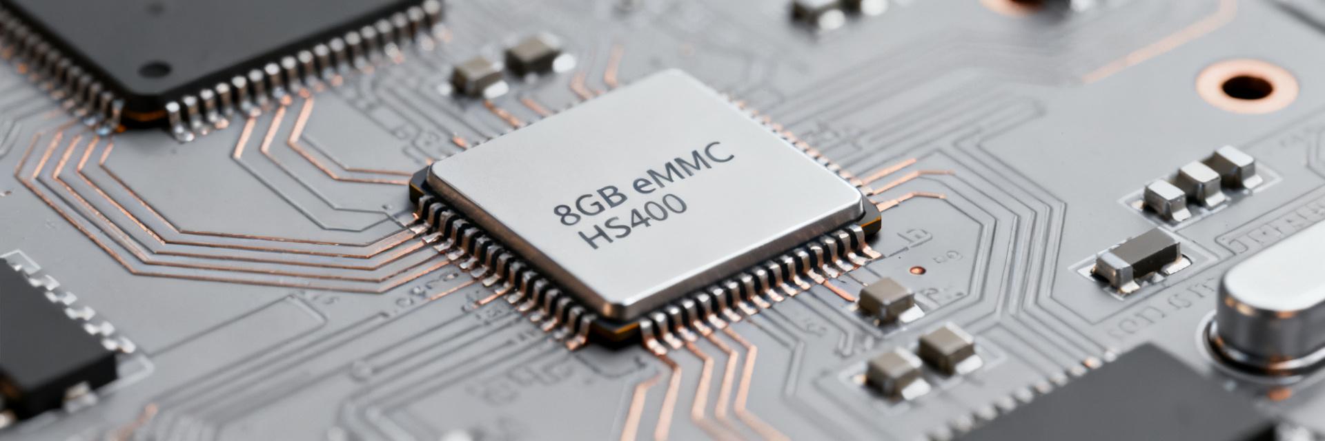
Form factor, package & pinout
Confirm package outline, thickness and ball/land pattern early in PCB release. Typical eMMC module drawings list overall length/width, maximum thickness and solder land pattern with recommended footprint tolerances. Verify the datasheet mechanical drawing for recommended PCB pad sizes, solder mask keepout, and maximum PCB warpage allowances. Follow the reflow profile guidance from the datasheet and keep mechanical tolerances conservative where the module abuts connectors or shielding.
Electrical specs & supported voltages
Check supported rails (1.8 V core and selectable 3.3 V I/O modes are common) and VIO tolerance margins; include recommended decoupling (multiple 0.1 µF and 1 µF caps close to supply pins). The module conforms to the eMMC 5.1 signaling and power conventions—verify absolute max ratings, recommended operating ranges, and any separate VCCQ sequencing notes. Also confirm operating temperature options (commercial vs. extended/industrial) and the specified maximum junction temperature in the datasheet.
KLM8G1GEUF-B04P: Performance benchmarks & throughput (Data analysis)
Sequential & random throughput (expected vs. theoretical)
HS400 theoretical interface bandwidth is ~400 MB/s; datasheet sequential read/write entries and random 4K IOPS provide expected device-level performance. Use standard tooling (e.g., fio or a validated host test harness) with defined IO sizes, queue depths and ambient conditions to reproduce numbers. Below is a concise comparison template engineers should populate with datasheet and measured bench results.
| Metric | Datasheet | Measured (bench) |
|---|---|---|
| Sequential Read (MB/s) | up to ~400 | --- |
| Sequential Write (MB/s) | datasheet value | --- |
| Random 4K R/W (IOPS) | datasheet R/W IOPS | --- |
Power profile & thermal performance
Datasheet active/read/write currents versus standby and sleep modes determine power budgeting. Measure power-per-MB by sweeping sustained write/read throughput and recording current at specified VCC/VCCQ. For thermal planning, expect surface temperature rise under sustained writes; allocate PCB copper as a heat spreader and add thermal vias beneath the module if sustained throughput is expected. Document power vs. throughput curves for system-level tradeoffs.
Reliability, endurance & data integrity (Data analysis)
Endurance metrics & retention (8GB eMMC context)
For an 8GB eMMC compute lifetime by combining P/E cycle endurance (datasheet P/E rating), expected daily write volume, and wear-leveling efficiency. Example method: annual written bytes / device capacity = rewrites per year; divide rated P/E cycles by that factor, adjusted for reserve/over-provisioning, to estimate years in field. Include expected data retention spec at end-of-life per the datasheet when planning backup and OTA strategies.
Firmware features: ECC, wear-leveling & bad-block management
On-module ECC, logical-to-physical mapping, over-provisioning and background garbage collection are primary mechanisms that preserve data integrity and steady-state performance. Verify the datasheet or firmware notes for support of TRIM/UNMAP, secure erase, boot partition handling and bad-block reporting. Confirm the module’s ECC strength and whether host-side tuning (e.g., retry policy) is required for your workload.
Integration & PCB design checklist (Method / how-to)
Power sequencing, decoupling & layout rules
Enforce required VCC/VCCQ sequencing to prevent latch-up: follow datasheet-specified order and timing. Place decoupling close to module power pins (0.1 µF ceramic + 1 µF or larger bulk caps), add ferrite if needed for EMI, and ensure solid power planes for low impedance. If the system toggles between 1.8 V and 3.3 V I/O, design or specify level translators and confirm VIO absolute max values.
High-speed signaling & HS400 signal integrity tips
Route CLK and data strobe with tight length matching, controlled impedance (typically 50 Ω single-ended or 100 Ω differential where applicable), and avoid stubs on high-speed lines. Use matched pairs for strobe/data, minimize via count, and place termination per datasheet guidance. A four-layer stack with referenced signal layers and dedicated ground/power planes is a common practical choice for HS400 designs.
Typical use cases & application guidance (Case examples)
Mobile & consumer embedded devices
An 8GB eMMC is often selected for compact OS plus application storage where cost, power and footprint are constraints. Expect strong sequential read performance for app load times, moderate write throughput for updates, and constrained random IOPS relative to higher-end flash; plan partitions for boot, userdata and cache to isolate wear and optimize performance.
IoT, industrial & automotive-adjacent deployments
For extended temperature and vibration environments, confirm the datasheet’s temperature grade and mechanical robustness. Implement OTA strategies that minimize sustained writes during updates, and validate retention and power-loss recovery under thermal cycling and vibration. Define test scenarios that mirror field conditions for realistic qualification.
Procurement, validation & testing playbook (Actionable steps)
Sample validation checklist (benchmarks & acceptance criteria)
Bench validation should include sequential/random benchmarks, power vs. throughput curves, sustained write stress, data retention checks, boot timing and power-loss recovery. Define pass/fail thresholds up front (e.g., sustained write throughput within X% of datasheet, no uncorrectable read errors after stress). Request formal datasheet version and test reports from the supplier to corroborate sample behavior.
Long-term qualification & firmware/driver notes
Recommend multi-week burn-in, field-aging tests, and CI inclusion for driver/firmware regressions. Validate host driver timing parameters, RPMB and boot partition behavior, and include filesystem corruption tests after power-loss cycles. Document test artifacts and failure modes to inform supplier change-control reviews.
Summary
- Confirm mechanical footprint and reflow guidelines from the official datasheet before PCB finalization to avoid assembly issues and ensure thermal compliance.
- Populate the datasheet vs. bench table for sequential read/write and 4K IOPS; use controlled fio workloads at defined queue depths to reproduce results reliably.
- Compute endurance using rated P/E cycles, expected daily writes and wear-leveling efficiency for an 8GB eMMC to determine field lifetime and backup cadence.
Frequently Asked Questions
What are the recommended benchmark conditions to validate throughput?
Use consistent IO sizes (e.g., 128K for sequential, 4K for random), defined queue depths (QD1–QD32 depending on target workload), and repeatable thermal conditions. Run multiple passes, log ambient and module temperatures, and capture power concurrently to analyze power-per-MB tradeoffs.
How should a team verify power-loss recovery and data integrity?
Perform power-fail tests during active writes and filesystem operations, then verify bootability and file integrity after simulated brownouts. Combine these with long-term retention tests and ECC error monitoring to confirm the module’s reported resilience.
Which production artifacts should procurement request from the supplier?
Request the exact datasheet version used for qualification, sample test reports (benchmarks, power, retention), and a declaration of firmware features (ECC level, TRIM support, boot partition handling). Keep these artifacts in the device qualification dossier.
What are the layout and routing rules for the HS400 high-speed interface?
Route CLK and data strobe with tight length matching, controlled impedance (typically 50 Ω single-ended), and minimize via count. Use matched pairs for strobe and data, and place decoupling capacitors (0.1 µF and 1 µF) as close to VCC/VCCQ pins as possible to prevent latch-up.